 |
|
| |  |
 |
|
|
|
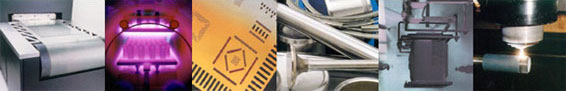
CHEMICAL VAPOUR DEPOSITION (CVD)
The many processing variants of CVD can be categorised as one of following base techniques:
thermal CVD:
* HTCVD (High Temperature CVD)
* APCVD (Atmospheric Pressure CVD)
* LPCVD (Low Pressure CVD)
plasma CVD
photo CVD
In CVD technology one works with gaseous starting material and the desired coating material is deposited as a result of a chemical reaction in the gas phase.
 |
 |
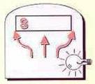 |
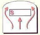
| Thermal CVD |
Plasma CVD |
Photo CVD |
The gas molecules react after supply of energy in the form of heat radiation (Thermal CVD), by incorporating them in an electric plasma (plasma CVD) or by activation with electromagnetic radiation (Photo CVD). CVD is a multi-purpose technique with which all materials on an atomic or molecular basis, are built as a layer, atom by atom or molecule by molecule.
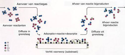
Aanvoer of reactiegas= Supply of reactive gases
Aanvoer reactanten= Supply of reactants
Diffusie in grenslaag= Diffusion in boundary layer
Adsorptie>reactie>desorptie= Adsorption>reaction>desorption
Verhit voorwerp (substraat)= Heated component (substrate)
Afvoer van reactie bijproducten= Removal of reaction side products
Diffusie uit grenslaag= Diffusion out of boundary layer
Afvoer reactie bijproducten= Removal of reaction side products
Schematic description of the many process steps which can be distinguished in a thermal CVD process.
It is not only possible to deposit very pure material, but one can also incorporate other phases in the growing layer. In this way layers with very fine - tuned properties can be manufactured, of which the morphology, composition, cross-section, and texture are controlled. By establishing other process conditions (for example other temperature and concentrations of the reactive substances in the gas phase) a clear difference in composition and morphology is seen, for example, in case of silicon carbide (Si C) growth on graphite. The result after treatment B is a more coarse morphology and texture than after treatment A.
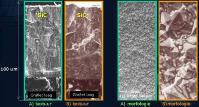
Cross section of CVD Si C on graphite. Surface of Si C-layer.
The deposition of multiple layers is no problem. Good examples of deposition materials are carbon, silicon and their compounds, and carbides, nitrides and oxides of several elements. The most important advantage of CVD compared to other thin film techniques is its capacity to grow layers of uniform thickness on very complex forms. CVD reactors can be stacked with components for mass production, and a large flexibility concerning form and dimensions of products is offered.
 |
 |
Fracture surface of alternating layers of
silicon oxide and tantalum oxide on a
quartz glass substrate. |
0.1 µm thick silicon oxide layer on a profiled silicon surface. |
 |
 |
Compact loading of a CVD reactor with machining parts to be deposited with
a gold coloured titanium nitridelayer. |
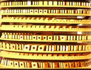
Mass production of yellow car lamps with a cover built out of 11 layers, which together form an interference filter. |
Chemical Vapour Deposition (CVD) - More information
Pierson: Handbook of Chemical Vapor Deposition, principles, technology and applications. Noyes Publications, Park Ridge, New Jersey, USA. (ISBN 0-8155-1300-3), 1992
Vossen/Kern: Thin Film Processes II. Academic Press, Inc., Harcourt Brace Jovanovich, Publishers.
(ISBN 0-12-728251-3), 1991
Bunshah: Deposition Technologies for Films and Coatings, Developments and Applications. Noyes Publications, Park Ridge, New Jersey, USA. (ISBN 0-8155-0906-5), 1982
Morosanu: Thin Films by Chemical Vapour Deposition. Elsevier. (ISBN 973-31-0228-8), 1990
B G Mellor, ed., Surface Coatings for Protection against Wear. Woodhead Publishing Ltd., Cambridge, UK. (ISBN 978-1.85573-767-9), 2006. chapter 3, 4 & 5.
Photo CVD
Laser or Photo CVD is based on the phenomenon that absorbed ultraviolet and visible photons frequently have enough energy to break chemical ties in molecules. Because of this growth processes can take place which are mainly based on the photolytic interactions with molecules in the gas phase or in an adsorbed layer on the substrate. Photo CVD differs from thermal laser CVD because no heat is necessary for the chemical reaction, as a result of which uniform layers can be deposited at very low temperatures. The industrial interest for the technique is low because of the low deposition rates.
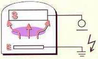
Plasma CVD
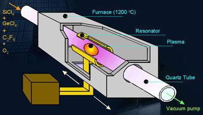
Plasma CVD (PECVD, plasma enhanced or PACVD, plasma assisted) offers the possibility of growing layers at relatively low temperatures (100 up to 650 °C).
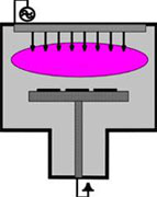
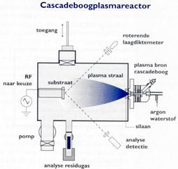
A schematic picture of a plasma CVD reactor.
 |
|
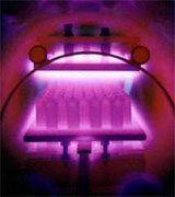
A picture where substrates in plasma are visible. A plasma, also called the fourth condition of matter (after solid, liquid and gaseous), is defined by Chen as a quasi-neutral gas of charged and neutral particles which show a collective behaviour. The relatively low temperatures in a plasma make possible a wider choice of substrate materials (e.g. plastics) and a broadening of application areas (among other things semiconductors). In plasma CVD a chemical process is combined with a physical process and as a result, the gap between CVD and PVD is to some extend bridged. Plasma CVD and reactive sputtering (PVD) are very similar.
Hybrid techniques of CVD and PVD are also applied. |
In the plasma CVD technique different alternatives are distinguished, depending on the nature of the plasma used. These include ' direct current ' (DC) for example with a Cascade plasma, ' radio frequency ' (RF), ICP and ' alternating current ' (AC), also micro-wave plasmas are used, pulsed or not.
Even in the deposition of diamond layers there are already several variants of plasma CVD. The same applies to diamond - like carbon layers (DLC), which are interesting because of their tribological and optical properties.
|
|
With the Cascade plasma CVD technique a large quantity of material can be deposited per unit of time.
Translation in figure:
Toegang= Entrance
Roterende laagdiktemeter= Rotating layer thickness meter
RF naar keuze= RF source
Substraat= Substrate
Plasma straal= Plasma beam
Plasma bron cascadeboog= Plasma source cascade
Argon= Argon
Waterstof= Hydrogen
Pomp= Pump
Analyse residugas= Analysis residual gas
Silaan= Silane
Analyse detectie= Analysis detected gases |
A micro-wave plasma is used for the deposition of a very large number of thin Silicon oxide layers for the production of starting material for optical fibres.
Chemical Vapour Deposition (CVD)
CVD can be carried out both at atmospheric and at lower pressure (0.1 to 10 mbar).
Usual deposition temperatures for Thermal CVD are 400 to 1050 ºC, for Plasma CVD 100 to 650ºC and for Photo CVD room temperature and higher.
With respect to starting material, layer composition and applications, CVD processes exhibit a large variety:
For high-temperature thermal CVD generally metal halogenides are used as starting materials.
In low-temperature processes less stable starting materials, such as organometal compounds, are used.
In IC production, generally CVD processes are used which lead to the deposition of semiconductors such as silicon, or compounds of silicon.
For tribological applications where controlled friction and wear are essential, mainly carbides and nitrides, which exhibit good mechanical (hardness, wear resistance, friction) and chemical (corrosion resistance) properties are used.
Chemical Vapour Deposition (CVD) Thermal CVD
|
|
Thermal activation of gaseous components is one of the basic mechanisms in many CVD processes.
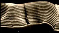
'High Temperature' CVD (HTCVD), in most cases carried out at temperatures between 800 and 1050 °C, is very common for the fabrication of powders, wires and bulk materials.
For the production of bulk materials such as chromium and silicon, very thick layers of the material are deposited on a hot wire which is then processed.
|
The figure shows part of the equipment for the continuous deposition of boron- or silicon carbide on a moving hot wire. The resulting wires are used for the reinforcement of epoxy composites.
|
|
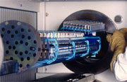
A similar method is used for the fabrication of various shaped parts such as hollow cylinders and crucibles made of boron nitride and tungsten in the following way:
On a pre-formed shape as base, a very thick layer is deposited, which is strong enough to act as a free-standing part after removal of the base. |
Boron nitride crucibles are producing starting with a preformed base material.
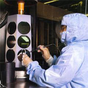
For the deposition of thin layers in most cases, the products are placed or hung in a closed reactor vessel.
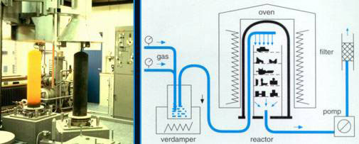
Schematic and photographic impression of a High Temperature CVD installation.
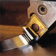
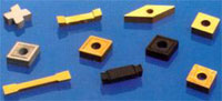
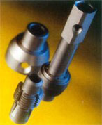
The coating of hard metal cutting tools (which can be bought in a large variety of composition and shapes) has become a very important industrial application of CVD, over the last sixty years. As hard, wear resistant and corrosion resistant coatings titanium nitride (Ti N), titanium carbide (Ti C) or aluminium oxide (Al2O3) are preferred, as separate coatings, or in combination.
 |
 |
|
Hard metal cutting tools covered with a hard coating of titanium carbide (grey colour), titanium nitride (gold colour) and aluminium oxide (black) often are applied in combination. A quickly growing application area is the coating of steel tools and machine parts with these hard layers. |
|
|
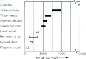
Comparison of the microhardness of some CVD layers (black) with a number of bulk materials.
As a very corrosion and oxidation resistant layer, chromium carbide (Crx Cy) can be mentioned, a material which can even be used up to 900°C in an oxygen containing atmosphere.
Translation:
Genitreerd staal = nitrided steel
Gehard staal = hardened steel
Ongehard staal = unhardened steel |
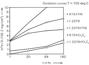
Oxidation resistance of CVD coatings on different substrate materials at 750°C.
In the deposition process the part to be coated is positioned in a CVD reactor, after which it is treated with a reactive gas mixture of chromium chloride (Cr Cl3) and a hydrocarbon compound such as butane (C4 H10). The carbon present in the substrate also takes part in the process of carbide formation.
 |
|
The chromium carbide layer, often denoted as Crx Cy, generally consists of three phases: Cr23 C6, Cr7 C3 and
Cr3 C2, of which Cr7 C3 is the most common. The composition of the chromium carbide is dependent of the composition of the underlying material.
Crx Cy layers are often being used in cases where a high oxidation resistance is required, as for instance in industrial burners. In cases where a high corrosion resistance is required chromium carbide is also applied, an example is moulds for glass forming.
Process temperatures of 850 to 900 °C are usual in practice, which results in deposition rates of 0,5 to 2µm per hour, depending on the process conditions and the composition of the (steel) substrate. The layer thickness increases linearly depending on process time. |
Insert pins of heat resistant stainless steel with a 5 to 10 µm thick layer of chromium carbides. The function of the layer is to decrease oxidation of the mould and as a result to prevent of the contamination of glass products.
Another application is the coating of graphite parts used in semiconductor fabrication. Barrier layers of silicon carbide are deposited on the parts in order to ensure high temperature stability, a high corrosion resistance and optimum purity of the semiconductor layers and substrate materials.
|
 |
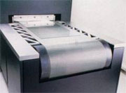
| Conveyorised APCVD system for the deposition of thin layers on flat surfaces (see the glass plate). |
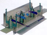
In a double loop recirculation system uniform and mechanically reinforcing (tin oxide) layers are deposited on bottles. |
Atmospheric Pressure CVD (also called conveyorised APCVD) is used as a cheap technique for the deposition on large surface areas. These continuous techniques are applied at atmospheric pressure and generally in a temperature range between 400 to 700 °C.
This technique has the advantage that the deposition rates are high and that each product is being subjected to the same processing cycle, which minimizes changes in properties.
An interesting application area is the coating of glass bottles with on on-line deposited hot-end coating (500°C) of tin oxide, which prevents the forming of micro - cracks on the glass surface and is an excellent adhesion layer for a thin poly-ethylene anti-scratch layer which is subsequently applied (cold-end coating deposited at 100°C).
'Low Pressure' CVD (LPCVD) enables deposition in a batch production situation of layers with a very uniform thickness, in low pressure (0.1 to 10 mbar) processes in a broad temperature range (400 to 900 °C).
|
|
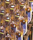
The positioning of car lamps in a LPCVD reactor |
|
|
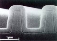
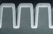
The unique possibility of CVD processes to deposit uniform layers on complex shapes is also seen in the Atomic Layer CVD (ALCVD) technique. The figure shows a 200 µm thick layer of aluminium oxide on 2 µm deep grooves in silicon.
ALCVD has recently been introduced in semiconductor fabrication and works at a pressure of 5 to 15 mbar in a temperature range of 100 to 500°C.
This technique, based on a sequence of reactions taking place at the surface, enables the deposition of very uniform, very thin (< 5 nm) and very dense layers for a number of potential applications, such as the production of ICs and displays. |
Schematic drawing of one ALCVD reaction period.
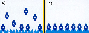
Vapour A is adsorbed at the surface which is already covered with atom B (a).
After saturation the surface is covered with atom A and again susceptible for the adsorption of atom B (b).
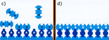
Excess vapour A is removed. Then adsorption of vapour B takes place, again until the complete surface is covered again (c) and a new cycle of adsorption starts again (d). In this way very thin layers are formed.
The so-called Thermal Laser CVD (LCVD) is a technique where the laser beam very locally hits the surface, generates heat and causes a thin layer to be deposited. The wavelength of the laser is chosen in such a way that no or very little energy is absorbed by the gas molecules.
However, the interest in this technique in semiconductor processing has not grown, since the rate of laser writing is not high enough.
An excellent adhesion between layer and substrate is characteristic for all thermal CVD techniques.
Applications
The fabrication of powders, components and thin layers are the most important application areas of CVD.
Thin CVD layers enable a number of important industrial applications.
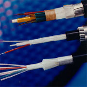
Glass fibers for optical communication which have been coated and integrated into a cable.
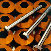
A wear resistant titanium nitride layer on a mould for the production of bolts increases the life expectancy of the bolt by a factor 4 to 7.
The fabrication of integrated circuits (ICs)
The electrical circuit with transistors, resistors and diodes after a large number of processing steps (CVD treatment and others) on a silicon wafer (dimensions 1 to 50 mm2)
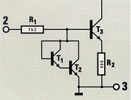
The electrical circuit
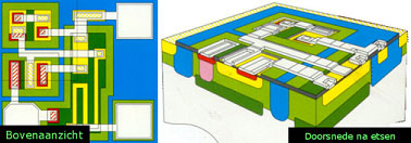
Seen from above Cross section after etching
An example of the one chip TV which controls the majority of functions in a colour television.
Coated graphite parts for use in the semiconductor industry
|
|
During IC production, Silicon wafers are positioned on a graphite carrier which has been coated with a 100 µm thick silicon carbide layer. This material is very corrosion resistant, dense and pure so that no impurities from the graphite can diffuse into the silicon. |
Protective layers on glass bottles.
Right of figure 7 NO PIC
Bottles are coated with a layer of tin oxide using APCVD to prevent microcracking in the glass surface. The tin oxide is then coated with a thin scratch resistant layer of polyethylene.
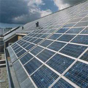
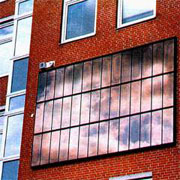
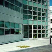
Solar cells and building windows, the so-called 'architectural glass.
 |
 |
Polycrystalline silicon solar cells are
coated with a titanium oxide anti-reflection layer. |
Amorphous silicon deposited by Plasma CVD is used in solar cell applications |
 |
|
Reflecting glass surfaces are used to reduce the heat generated by incident sun light. Glass surfaces are covered by silicon oxide and tin oxide using continuous CVD processes at atmospheric pressure. |
|
|
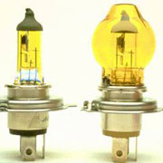
The old and the present design situation for car lamps. Right the old situation where cadmium is used in the yellow light transmitting glass container. Left the new situation where an eleven layer filter of 0.8 µm thickness, of alternating silicon oxide and silicon nitride layers, is deposited on the lamp. Optical interference filters made using CVD are a new technological advance in the production of lamps. |
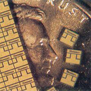
Illustration of the size of laser cut pieces of polycrystalline diamond (compare to the coin)
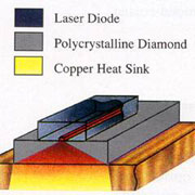
The effect of heat transmission enables the use of higher powers, the temperature of the diode remains relatively low.
|
|
An optically transparent 2µm thick diamond membrane is produced by Microwave Plasma CVD on a silicon wafer with a diameter of 10 cm.
Next the central part of the wafer is etched away, so that a free-standing membrane is left.
|
|
|
|
|
|
|
|