 |
|
| |  |
 |
|
|
|
DECORATIVE COPPER PLATING
1. Introduction
Electrolytic copper is deposited on a product (as cathode) using direct current. An aqueous solution of copper salts and copper metal as anode are applied. Special organic additions are used to obtain decorative coatings and a good spread on the substrate surface.
|
|
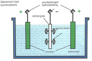
Schematic picture of an electroplating bath
Terms in Figure:
Galvanisch bad (schematisch) = Galvanic bath (schematics)
Anodestangen = Anode pole
Kathdesrang = cathode pole
Ophangrek = suspension grid
Werkstukken = products
|
2. Properties
Copper layers are very decorative and good electrical conductors. Depending on additions hardness can vary between 90 HV and more than 200 HV.
Copper layers are not very wear resistant and may tarnish when touched. For functional applications a copper layer is often covered by another metallic layer or in some cases an organic top coating.
3. Substrate
The most usual substrates are plastic (activated by special pretreatment) and zinc. Also brass, unalloyed or low alloyed steel and aluminium are used.
4. Process characteristics
Electrolytic copper deposition is carried out in an aqueous solution of copper salts. The following baths are used:
- strong acid copper baths
- cyanide strong alkaline copper baths
- cyanide free, mildly alkaline copper baths
The strong acid baths, based on copper sulphate and sulfuric acid, are most common. These baths generate bright layers with good coverage.
Cyanide baths contain Cu (I)cyanide, alkaline cyanides and are primarily used for electroplating of zinc, sometimes in combination with acidic copper. A cyanide based pre - copperplate bath is always used (copper strike) in order to prevent contact copper (displacement deposit). This type of process normally gives less bright layers.
Cyanide free, pyrophosphate based layers can be used in all cases where cyanide and acid baths are applied. The brightness and coverage are generally less good than in case of acid baths.
Pretreatment
The substrate should be absolutely free of oil, grease or an oxide layer. The following process steps are generally required:
- degreasing in a solution (alkaline and water-based)
- rinsing
- pickling
- rinsing
- electrolytic degreasing (alkaline and water-based)
- rinsing
- activation
- rinsing
- copper strike, cyanide based
Special substrate materials, such as plastics, plastic laminates and aluminium require a special pretreatment.
Layer deposition
The components are immersed in the copper solution and connected to the negative electrode (cathode). Small parts and/or large runs are treated in barrels.
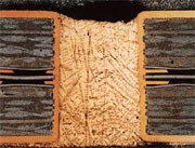
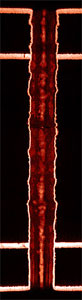
Cross section of a copper plated printed circuit board
Depending on the current density distribution at the surface of the part, the layer will be formed in a more or less uniform way. Layer thicknesses of 5 to 25 µm are common for most functional applications. On pressure printing cylinders and in case of electroforming layer thicknesses of hundreds of µm are common. See also ISO 1456; ISO 4525.2
5. Advantages and disadvantages
Advantages
- copper layers have an excellent heat and electrical conductivity
- a very wide range of properties is possible (by changing the deposition conditions)
- applicable on a large number of materials and plastics, which can easily be plated with copper
- copper plating is an essential step in the fabrication of printed circuit boards
Limitations
- copper may tarnish in air or when touched. This necessitates a metallic or organic top layer
- layer thickness depends on the current density, which limits the forms which can be copper plated. For copper plating as such, a cyanide based copper strike before the electrolytic plating is always needed in order to prevent contact or exchange Cu. (displacement deposition).
6. Applications
In former times copper plating was most common as a first layer in the electroplating of steel plates. Nowadays, the most common applications are in electronic components (printed circuit boards), the metallising of plastic, zinc pressure castings and electroforming.
| |
|
Cross section of a copper plated printed circuit board |
|
|
The copper through metallising of holes in printed circuit boards.
Also used in rotation printing on printing cylinders. |
|
|
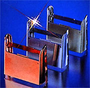
An important application of electroplated copper is as first layer in electroplating in general. In this example the first layer is copper, the second is nickel, the top layer is chrome. |
 |
|
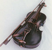
Bronze copy of a violin. The wood is made electrically conductive after which copper plating and a bronze layer (Cu-Sn) were deposited. After that the metal layer is separated from the wooden substrate. During metallising of organic substances, such as wood, plant components and plastics, or on glass, copper is always used as a first layer. The reason is that most electroplated materials adhere very well on copper. |
|
|
|
|
|
|
|