 |
|
| |  |
 |
|
|
|
ELECTROLYTIC LEAD-TIN
Introduction
Electrolytic lead-tin is an alloy which can be deposited in varying compositions between the extremes 95% tin /5% lead to circa 60% tin /40% lead.
In this last, so-called eutectic composition, the alloy has a minimum melting temperature which is lower than the melting point of both constituent metals.
Lead-tin plating is carried out in an aqueous, acid solution, in which tin and lead salts are present in a desired ratio. As anode the same material which is deposited can be used. The product is connected to the cathode. Due to the difference in nobility between lead and tin, organic additions are necessary for control of the metal ratio in the layer and for control of the crystal structure.
Properties
The tin-lead (or lead-tin) layer is dense, fine crystalline, dull grey. Tin-lead is very soft and vulnerable to scratches and abrasion.
Substrate
For PCB applications copper is always the substrate. Lead-tin protects the copper against etching chemicals.
In connector applications also copper is used.
Process characteristics
Common processes are based on methylsulphonic acid (MSA) or fluoroboric acid. MSA processes are the most expensive but more reliable since they form the insoluble Tin(IV)oxide and have a more dense layer structure. Also the MSA based baths are less aggressive for equipment and environment.
Pretreatment
An acid dip right after copper electroplating is sufficient. On older copper it is needed to pre-etch the material.
Plate material needs to be degreased (in a alkaline solution) and then activated
Layer deposition
The tin-lead is deposited on cathodically connected parts with electric currents between 1 and 2 A/dm2. Temperature is between 20 and 23C.
The process efficiency is between 85 - 95%, depending on process conditions.
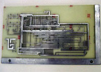
During PCB fabrication, the lead-tin is deposited on an electrolytic copper layer. The lead-tin acts as etch resist during etching of resist film and superfluous copper.
Depending on the desired finish the tin-lead layer can be removed or melted for the creation of a solderable protective layer against oxidation. Lead-tin deposition on electronic components, e.g. connector band, is carried out in a continuous system with higher current densities (up to 30 A/dm2). In these cases a lead rich tin-lead alloy is deposited.
 |
 |
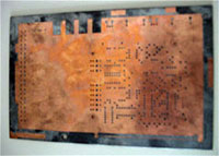
Print plate with an electroplated
tin-lead coating |
After treatment
No specifications |
Advantages and disadvantages
Advantages
- tin-lead has a broad application range, since it is used as etch resist, base material for soldering, and as oxidation protection
- in contrast to tin, tin-lead deposits can easily be melted
Disadvantages
- Lead is less advantageous for environmental protection and health reasons
In Japan, lead is already banned in PCBs, in Europe this will be the case starting from 2008.
Cost
Cost strongly depends from the process (fluoroboric acid or methylsulphonic acid). Cost also depends on the layer thickness
Applications
Electrolytic tin-lead is a functional coating, applied as etch resist on PCBs and as solderable coating on electronic components.
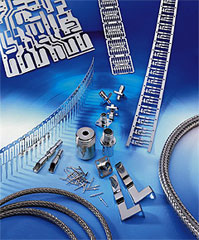
Electronic components with a tin-lead coating
Brush plating
In brush plating the electrolyte is pumped through a brush or pad in contact with an anode (usually insoluble carbon). The work - piece is made cathodic as a low - voltage d.c. is applied. This technique is useful for the localized electroplating of objects that are too large for conventional plating tanks or to restore articles that are not easily disassembled. It is also applied when deposition is required on limited areas.
Further information may be obtained from www.sifcoasc.com
Pulse plating
In pulse plating the normal direct electroplating current is interrupted, usually τon + τoff < 1 sec, τon is greater than 10 msec. Periodic reverse pulse plating involves a short but intense anodic pulse, in the cycle. Modern plating controllers use microelectronics to obtain precise pulse control, giving significant improvements in some plating processes. These techniques are used particularly in the printed circuit board industry to avoid the use of addition agents which can cause impurities especially in the deposition of copper and silver, also to reduce plating lines and to increase production capacity.
For further information go to www.instct.org, peter.leisner@sp.se or P T Tang at tt@ipl.dtu.dk
|
|
|
|
|
|
|