 |
|
| |  |
 |
|
|
|
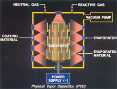
PHYSICAL VAPOUR DEPOSITION (PVD)
Although many different names are given to the various process variants of PVD all processes can be categorized into the basic techniques:
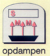
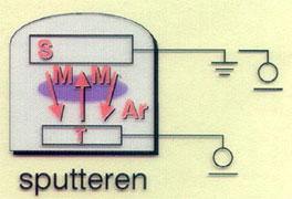
Vapour deposition and Sputtering
Evaporation:
- Ion Plating
- Arc Deposition
Sputtering:
In PVD technology (thin) layers on a substrate are formed by condensation of atoms or molecules from a gas or vapour. This is a different process than CVD where material is deposited from the gas phase by a chemical reaction on the substrate surface. In the physical methods the starting material is always transported into the gas phase from a solid state target in the reactor. In some of the PVD techniques reactive and/or non-reactive gases are also added.
 |
 |
| Evaporation |
Sputtering |
Depending on the evaporation method the following basic techniques can be discerned: Evaporation and Sputtering.
A characteristic of PVD technology is that the techniques are carried out in vacuum.
The technology can be considered as clean since in principle the whole process is executed in a closed system. PVD is a so-called line-of-sight deposition technology this in contrast with CVD which is a volume deposition technology.
This means that there is a directional deposition effect in PVD: the particles which form the layer move from the target to the substrate. In order to reach a uniform deposition on a 3D form it is necessary to rotate the form in the reactor, so that all surfaces are reached by the evaporated particles. The necessity to rotate is at the expense of the reactor volume utilization.
|
|
In the PVD reactor (door is open) one can see the rotation table which carries the products during the deposition process.
PVD is a very versatile technique which makes it possible to deposit almost any type of inorganic material (metal, alloys and compounds) on an atomic or molecular basis as a coating. It is not only possible to deposit very pure substances, but also very well controlled quantities of third substances can be built into the coating.
In this way coatings with controlled properties such as composition, thickness, density and texture are made. |
|
|
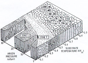
Schematic drawing of the influence of substrate temperature and argon pressure on the structure of metal layers, deposited by sputtering, using a cylindrical magnetron source.
T is the substrate temperature, Tm the melting point of the deposited material in degrees Kelvin. Zone T stands for transition Zone.
The deposition temperatures in PVD are relatively low so that a large variety of substrate materials can be used, such as polymers. The deposited material is most often a metal or metal alloy, or a compound such as a nitride, carbide or oxide. |
Introduction
- Simon/Thoma:
Angewandte Oberflächentechnik für metallische Werkstoffe. Carl Hanser Verlag München/Wien.
(ISBN 3-446-14221-5), 1985
- Frey/Kienel: Dünnschicht Technologie. Verlag des Vereins Deutscher Ingenieure Düsseldorf (VDI Verlag).
(ISBN 3-18-400670-0), 1987
- Vossen/Kern: Thin Film Processes II. Academic Press, Inc., Harcourt Brace Jovanovich, Publishers.
(ISBN 0-12-728251-3), 1991
- Bunshah: Deposition Technologies for Films and Coatings, Developments and Applications.
Noyes Publications, Park Ridge, New Jersey, USA. (ISBN 0-8155-0906-5), 1982
Refer to Teer Coatings Ltd : www.teercoatings.co.uk
Evaporation
During evaporation, the target material may be evaporated in several ways, e.g. by direct or indirect heating with an electrical current, or by using an electron beam.
Of course, only materials with a sufficiently high vapour pressure can be used in evaporation.
The technique is best suited for pure elements, compounds are more difficult. The substrate is at zero potential normally, so there is no potential difference with the target material. The evaporated material condenses on the substrate. This simple and well known technique generates porous coatings, with a decreased adhesion to the substrate, especially at higher deposition rates.
|
|
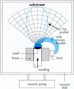
Evaporation process using an electron beam
Vacuum pump
Vacuum clock
Melted material
Crucible
Source
Electron beam
1 Lux profile
Substrate
When a reactive gas is added, which reacts with the evaporated material, the process is called reactive evaporation.
|
 |
|
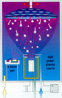
Ion plating
Schematics of an Ion Plating process where electron beam evaporation is used and the ion bombardment leads to good coating properties. |
During ion plating the coating material is also evaporated. Here one tries to combine the high evaporation and condensation rates with superior coating characteristics, such as adhesion, density and microstructure. This is achieved by the ion bombardment on the substrate. Higher overall pressures are used than in the case of simple evaporation.
Arc evaporation
During arc evaporation another technique of evaporating the target material is used: the material is evaporated using an electric arc. Often multiple sources are placed in the reactor, in order to ensure a more uniform deposition. The Explosive evaporation can lead to the inclusion of micro-droplets in the coating material. By changing the arc position over the target material the number of micro-droplets can be limited.
The arc is a discharge with a higher ionization degree than that in ion plating, and it generally spreads through the reactor. In this way better adhering coatings are obtained.
Schematics of arc evaporation.
Processes
Deposition in PVD is always carried out at low pressures. Usual deposition temperatures are 100 to 500°C, depending on the requirements for the system substrate/coating.
Target materials are high purity depending on the application 99,9 to 99,999 %.
In IC fabrication, aluminium is generally used for the electrical contacts.
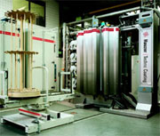
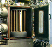
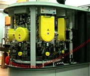
PVD installation with a large volume (Ø 900 mm x 1500 mm)
The use of aluminium is being partially replaced by copper. Chromium is used for few display fabrications. For decorative coatings, Ti N and compositions derived of Ti N are being used.
Sputtering
During sputtering the noble gas argon is added to the reaction chamber, and a high continuous voltage or rf voltage is coupled to the target material. This causes a gas discharge (plasma) between the source and the substrate(s). The argon ions generated in the plasma collide with the target material at high energy, and release free surface atoms from this material. These (neutral) atoms deposit as a thin layer on the substrate. An advantage of this way of creating a vapour phase is that materials which are very difficult to evaporate can be brought into the gas phase.
The deposition rates depend strongly on the target material and are generally lower than in case of evaporation. Another disadvantage is that the Ar ions are built into the coating material.
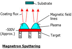
By analogy with reactive evaporation,' reactive' sputtering is when a reactive gas is used during sputtering. When magnetic fields are used to increase the effectiveness of the discharge, this is called magnetron sputtering. In this process electrons in the plasma cannot escape to the reactor wall. As a consequence, they are available for ionization during a longer time.
The technique enables deposition at lower pressures and the minimal incorporation of impurities. The deposition rate generally is low, so that deposition is often done at higher pressures. Also more complicated reactor configurations are used with magnetron sputtering. A good example is a reactor with 4 magnetron systems.
 |
 |
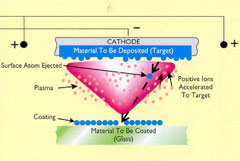
| Schematics of the sputtering technique, where it is shown that material is transported from the target to the glass substrate. |
Schematics of magnetron sputtering |
 |
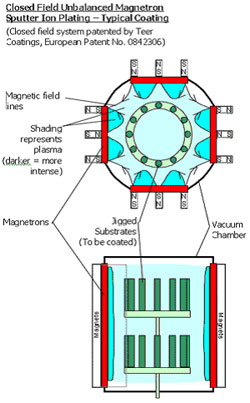 |
| A quadruple magnetron installation |
Schematics of the top and side view of a quadruple magnetron installation |
 |
|
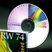
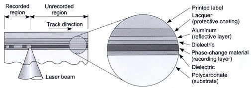
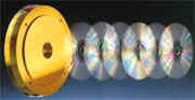
A clustered reactor where magnetron sputtering is used for the production of rewritable CDs and DVDs.
Here on a carrier material 4 consecutive layers are deposited: a Zn S-Si O2 mixture as anti-reflection layer, a In Sb Ag Te alloy as active layer (upon activation this layer changes from crystalline to amorphous), then another ZnS-SiO2 layer, and finally an aluminium layer as reflecting layer. |
Application
PVD layers are being used in a broad area of applications e.g.
In micro-electronics metals, aluminium is deposited to form electrically conductive layers, and the same metal ( as also copper ) is being used as reflection material on plastic information carriers, such as CD-ROMs.
|
 |
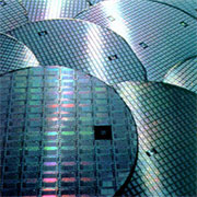
Silicon discs on which electrical contacts
in the form of patterns can be seen. |
CD-RW disc (RW=rewritable) |
A multilayer system on a CD-RW disc
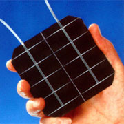
Solar cells and displays are metallised using PVD. The metal layer functions as an electrically conductive layer.
 |
|
Aluminium layer on a photovoltaic solar cell in the form of an electrical circuit.
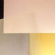
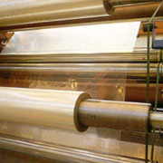
Also polymer foils are deposited with metals or oxide layers. This is carried out in the packaging industry on a large scale, foils are coated with air tight layers of silicon oxide. |
 |
 |
Different layers on foils: e.g. a electrically conductive layer of tin oxide (transparent)
and copper.
|
The coating of packaging foil is
carried out on a large scale.
|
The technique is widely applied in optics, opto-electronics, and sensor technology. Glass and polymer are coated with layers for applications such as in spectacle glasses, and sun glasses, lamps, colour filters, and laser or cold light mirrors.
 |
 |
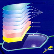
In order to make a scratch resistant and
anti-reflection layer on spectacle glass
multiple layers are used. |
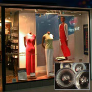
So called cold light mirror lamps
are used in shop windows. |
The coating of flat glass for windows in buildings and cars is an important optical application.
For cars a transparent electrically conductive layer is used to keep windows free of ice by ohmic heating. PVD is also used in the production of thermal barrier coatings on turbine blades.
|
|
Windows are often coated with so-called solar control architectural coatings. |
In cars a transparent, electrically conductive layer is used to keep the windows free of ice.
|
|
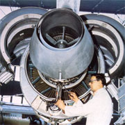
The turbine blades in front (furthest, seen from the cockpit) are covered with a PVD (EB-PVD: Electron Beam Deposition) heat isolating Zr O2 layer. Material temperatures of 1000oC are not uncommon in these applications. |
PVD also plays an important role in the deposition of nitrides and carbides for wear resistance and corrosion resistance applications.
 |
 |
Steel moulds are covered with
Ti N and are more corrosion
resistant so that their service life is longer. |
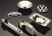
Coatings on automotive components
often have both functional
and decorative applications.
|
 |
 |
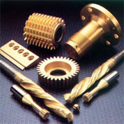
Cutting tools such as drills and milling tools
are also coated with wear resistant titanium nitride |
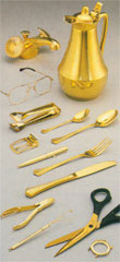
Different applications of
decorative layers. |
Decorative layers
A separate class of decorative layers is where very hard materials are used. Since various nitrides and carbonitrides can be deposited in different colours they are very suited as decorative layers. Their high hardness guarantees a high scratch resistance, also materials such as titanium nitride (Ti N), titanium carbonitride (Ti CN), chromium nitride (Cr N), titanium-Aluminium-nitride (Ti Al N), zirconium nitride (Zr N) and zirconium carbonitride (Zr CN) have a high corrosion resistance. As a result of the low deposition temperature polymers can also be metallised.
In brief, the following properties can be ascribed to decorative layers: a colour spectrum from yellow to violet, from metallic to black; hardness 1900-2800 HV0.05; in a scratch test with a diamond tip the layers are well adhering up to a critical load of 50 N; the layers are chemically resistant against alkali cleaning agents, and in a salt spray test; layer thickness is mostly between 0.5 and 2 µm; a temperature resistance up till 600ºC may be reached.
A large variety of materials can be used as substrates: steel and stainless steel alloys. Titanium, brass and Maillechort (also called New Silver - Argentane - Alpaca); sometimes an electroplated pre - coating of Ni-Cr of Ni-Pd-Ni is applied. Zinc with a coating of Cu-Ni-Cr and metallised polymers can be used.
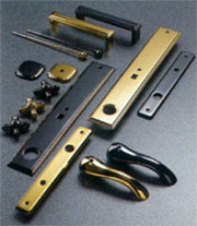
Door metal work
There are many applications of PVD decorative coatings. The most important are: metal work on doors and furniture, elements of banisters, railings and fencings, and coatings on utensils such as clocks, spectacles and pens; metallised polymer components of cars and coated car rims.
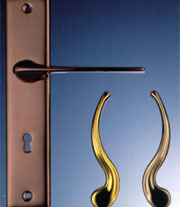
Door metal work can be made very decorative
by using different coloured coating materials.
|
|
|
|
|
|
|